Si2 Workshop Explores Global Effort to Measure AI Compute Capacity and Infrastructure

An international effort to assess artificial intelligence compute capacity and help governments make informed AI infrastructure investments is the focus of an online workshop hosted by Silicon Integration Initiative, January 29, 8:00-10:00 am PST.

Keith Strier, vice president, Worldwide AI Initiatives at NVIDIA, will discuss the AI Compute Task Force created in early 2020 by the Organisation for Economic Co-operation and Development. The OECD is a Paris-based intergovernmental economic group with 37 member countries, founded in 1961 to stimulate economic progress and world trade. The task force is developing a framework to measure and benchmark domestic AI compute capacity and other AI readiness components, including budgets and investment priorities.

Their work could also address concerns that wealthier countries are making outsized investments in AI compute capacity, possibly leading to a global compute divide that will sustain resource inequalities in a global digital economy. Strier chairs the OECD task force and has primary responsibility for the NVIDIA global public sector portfolio and the AI Nations Partnership Initiative. He also advises national and city government leaders on AI policies and infrastructure.

The workshop also features Yiorgros Makris from the University of Texas at Dallas. He will discuss how machine learning can reduce semiconductor testing costs, increase test quality, improve yield and test floor logistics, and guide designers and process engineers.

Makris is a professor of Electrical and Computer Engineering and co-founder of the NSF Industry-University Cooperative Research Center on Hardware and Embedded System Security. His research focuses on applying machine learning and statistical analysis to develop trusted and reliable integrated circuits and systems, emphasizing the analog/RF domain.

The workshop will conclude with an update on the Si2 AI/ML in EDA Special Interest Group. Speakers are Joydip Das, SIG chair and senior engineer, Samsung Austin R&D Center; and Kerim Kalafala, SIG co-chair and senior technical staff member, IBM EDA.

The workshop is open to the public and registration is free. For more information visit http://bit.ly/si2_ai_workshop.

About Si2

Founded in 1988, Si2 is a leading research and development joint venture that provides standard interoperability solutions for integrated circuit design tools. All Si2 activities are carried out under the auspices of The National Cooperative Research and Production Act of 1993, the fundamental law that defines R&D joint ventures and offers them a large measure of protection against federal antitrust laws. The Si2 international membership includes semiconductor foundries, fabless manufacturers, and EDA companies.

Si2 Launches Survey on Artificial Intelligence and Machine Learning in EDA

Si2 has launched an industry-wide survey to identify planned usage and structural gaps for prioritizing and implementing artificial intelligence and machine learning in semiconductor electronic design automation.

The survey is organized by a recently formed Si2 Special Interest Group chaired by Joydip Das, senior engineer, Samsung Electronics, and co-chaired by Kerim Kalafala, senior technical staff member, EDA, and master inventor, IBM. The 18-member group will identify where industry collaboration will help eliminate deficiencies caused by a lack of common languages, data models, labels, and access to robust and categorized training data.

This SIG is open to all Si2 members. Current members include:

  • Advanced Micro Devices
  • ANSYS
  • Cadence Design Systems
  • Hewlett Packard Enterprise
  • IBM
  • Intel
  • Intento Design
  • Keysight Technologies
  • Mentor, a Siemens Business
  • NC State University
  • PFD Solutions
  • Qualcomm
  • Samsung Electronics
  • Sandia National Laboratories
  • Silvaco
  • Synopsys
  • Thrace Systems
  • Texas Instruments

The survey is open April 15 – May 15.

The survey link is:  https://bit.ly/SI2_AI_ML_Survey

Leigh Anne Clevenger, Si2 senior data scientist, said that the survey results would help prioritize SIG activities and timelines. “The SIG will identify and develop requirements for standards that ensure data and software interoperability, enabling the most efficient design flows for production,” Clevenger said. “The ultimate goal is to remove duplicative work and the need for data model translators, and focus on opening avenues for breakthroughs from suppliers and users alike.”

“High manufacturing costs and the growing complexity of chip development are spurring disruptive technologies such as AI and ML,” Clevenger explained. “The Si2 platform provides a unique opportunity for semiconductor companies, EDA suppliers and IP providers to voice their needs and focus resources on common solutions, including enabling and leveraging university research.

SI2 Launches Special Interest Group For AI and ML in Electronic Design Automation

SIG Will Fill Industry Gaps to Enable Artificial Intelligence and Machine Learning in EDA

Silicon Integration Initiative has launched a special interest group to focus on the growing needs and opportunities in artificial intelligence and machine learning for electronic design automation.

The group will identify current solutions and technology gaps in AI and ML strategies for EDA digital design. “AI and ML are changing semiconductor design and improving performance and time to market,” said Leigh Anne Clevenger, Si2 design automation data scientist.  “Based on member company interest, we expect the SIG to propose prototype projects to accelerate the development of standards in areas such as machine learning training, and data handling and sharing.

“High manufacturing costs and the growing complexity of chip development are spurring disruptive technologies such as AI and ML,” Clevenger explained. “Si2 provides a unique opportunity for semiconductor companies, EDA suppliers and IP providers to voice their needs and focus resources on common solutions, including leveraging university research.”

The SIG is open to all Si2 members and is chaired by Joydip Das, Senior Engineer I, Samsung Austin R&D Center, and co-chaired by Kerim Kalafala, senior technical staff member, EDA, IBM.

“In recent years, the EDA industry has significantly expanded the use of AI/ML technology and techniques in its design tools,” said Das. “We’ve identified the need for a common industry-wide infrastructure to help share this information. This will help eliminate duplicative work and open up avenues for new breakthroughs.”

Other Si2 members participating in the SIG include: Advanced Micro Devices, ANSYS, Cadence Design Systems, Hewlett Packard Enterprise, Intel, Intento Design, NC State University, PDF Solutions, Sandia Labs, Synopsys and the University of California, Berkeley.

About Si2

Founded in 1988, Si2 is a leading research and development joint venture that provides standard interoperability solutions for integrated circuit design tools. Its activities include support of OpenAccess, the world’s most widely used standard API and reference database for integrated circuit design. All Si2 activities are carried out under the auspices of The National Cooperative Research and Production Act of 1993, the fundamental law that defines R&D joint ventures and offers them a large measure of protection against federal antitrust laws.

We Need Your Insights on How to Improve the IC Design Ecosystem

Silicon Integration Initiative (Si2) has launched a comprehensive, international survey to identify and address ways to streamline and improve the IC design ecosystem.

Survey results will be announced in a DAC 2018 white paper, whose contents will present an industry consensus on specific ways the industry can manage the rising costs of more complex designs and smaller geometries.

You can access the survey and share your insights here. It will take about 20 minutes to complete.

Si2 extends its thanks to the Electronic System Design Alliance for its support of this survey.

Thanks for sharing your expertise!

Complete the survey today! Amazon gift cards will be sent to the first 50 respondents.

Have Ideas on Improving the IC Design Ecosystem?

Si2 is seeking industry input on an international effort to identify and address ways to streamline and improve the IC design ecosystem. The finished product will be a DAC 2018 white paper whose contents will present an industry consensus on specific ways the industry can manage the rising costs of more complex designs and smaller geometries.

We’re looking for comments and suggestions on specific design concerns to include in an industry survey whose results will provide data for the white paper. IC designers and engineers can submit survey questions for consideration at https://lnkd.in/eJGgVQR.

If you have questions about the survey or white paper contact Ted Paone, [email protected].

Si2 Launches Effort to Improve IC Ecosystem

Si2 Launches Effort to Improve IC Design Ecosystem

New Special Interest Group Will Present Recommendations at DAC 2018

Si2 is seeking industry input on an international effort to identify and address ways to streamline and improve the IC design ecosystem. The finished product will be a DAC 2018 white paper whose contents will present an industry consensus on specific ways the industry can manage the rising costs of more complex designs and smaller geometries.

Ted Paone, Si2 interoperability standards architect, said the first step in the process was the formation of the Si2 Design Ecosystem Special Interest Group (SIG), which will write and distribute an industry-wide survey identifying areas of concern. The survey will launch in March 2018. Intel, Cadence Design Systems, Micron, Samsung, IBM and PDF Solutions are charter members of the SIG, which will investigate the impact of current issues in design and the expectations of future design requirements including performance and interoperability improvements to design data bases and scripting languages.

IC designers and engineers can submit survey questions for consideration at https://www.surveymonkey.com/r/9NSZCLC.

“We’re asking for the industry to help identify their specific design concerns so we can incorporate them into our survey,” he explained. “These are the people whose day-to-day activities are complicated by the need to create successful silicon while dealing with more and more complex processes, larger designs, new security and traceability issues, and emerging technologies such as chiplets, photonic elements and three-dimensional packaging.”

For information about the Si2 Design Ecosystem SIG, contact Paone, [email protected].  Information about joining the SIG is available at www.si2.org.

About Si2

Founded in 1988, Si2 is a leading research and development joint venture that provides standard interoperability solutions for integrated circuit design tools. All Si2 activities are carried out under the auspices of the National Cooperative Research and Production Act of 1993, the fundamental law that defines R&D joint ventures and offers them a large measure of protection against federal antitrust law.

EDA Scripting Unleashed (Voted-Best-Paper)

Author:  James Masters, Intel

In many traditional design flows, high-performance robust EDA capabilities are limited to formal EDA tools. Design Automation (DA) engineers build additional project-specific capabilities either by using an EDA tool’s proprietary scripting API or by creating a standalone lightweight script that relies upon translation of design data into other formats. This results in extra runtime overhead, additional possible points of failure, and a burden of working with lossy design data formats.

With the advent of oaScript, DA engineers can quickly write scripts that directly read and write OpenAccess (OA) data using one of their favorite scripting languages – Perl, Python, Ruby, or Tcl. Also, a new OA extension is now available which provides high-speed layer manipulation and boolean operations directly within an oaScript – called “oaxPop” (OA eXtension Polygon Operators).

The combination of oaScript with oaxPop enables a DA engineer to write high-performance robust EDA capabilities without the overhead of using a formal EDA tool. This presentation will demonstrate how oaScript and oaxPop have been used together to create real-life applications that are used in a production design flow.

BIO:

James Masterjames_master_1000x1000s graduated from the University of Phoenix with a Bachelor of Science in Information Technology with an emphasis on computer programming. He has worked at Intel Corporation for 20 years in various full-custom design implementation roles.

James is currently managing a team focused on improving custom layout productivity for Intel’s advanced process technologies. James is an advocate of open standards that help streamline the design flow and maximize productivity and reuse.

Outside of work James enjoys outdoor activities such as camping, fishing, hiking, gardening, etc.

Si2 Special Interest Groups—Forums for Collaborative Problem Solving

Ted


By Ted Paone
Si2 Interoperability Standards Architect

It is a new year but those design issues you could not fix last year are still robbing your company’s productivity. The problems didn’t stop at the beginning of this year, and there are less time and limited staff to find the solutions.  Well, you are not the only one. In my many years as a corporate application engineer for a large EDA company, I’ve heard the same stories told again and again, with slight variations and a different cast of characters. If I could only get them in the same room, we could discuss the insights to solve these common problems, but that could be collusion with all its consequences.

In 2017, you are no longer alone. The Special Interest Groups (SIG) set up under the anti-trust protection of Si2 allow you to solve design problems with other companies in the industry, sharing hundreds of years of knowledge of designers to address common issues. Si2, as a research and development joint venture, provides an opportunity to collaborate with like-minded companies to identify, document and even solve problems in the electronics/photonics design fields.

Within the Si2 structure, SIGs can be formed to address general or specific design topics such as Silicon Photonic/Electronic Co-Design, Process Design Kit Generation or Design Migration. The SIGs are the incubator for ideas within the Si2 structure. The SIG can create industry surveys to find and prioritize the issues and work with other industry groups to develop roadmaps. Members can jointly write white papers and present at conferences. Using the Si2 infrastructure, the SIG can spawn projects including prototyping implementations, developing standards and creating training and documentation.

sig-chart-copy
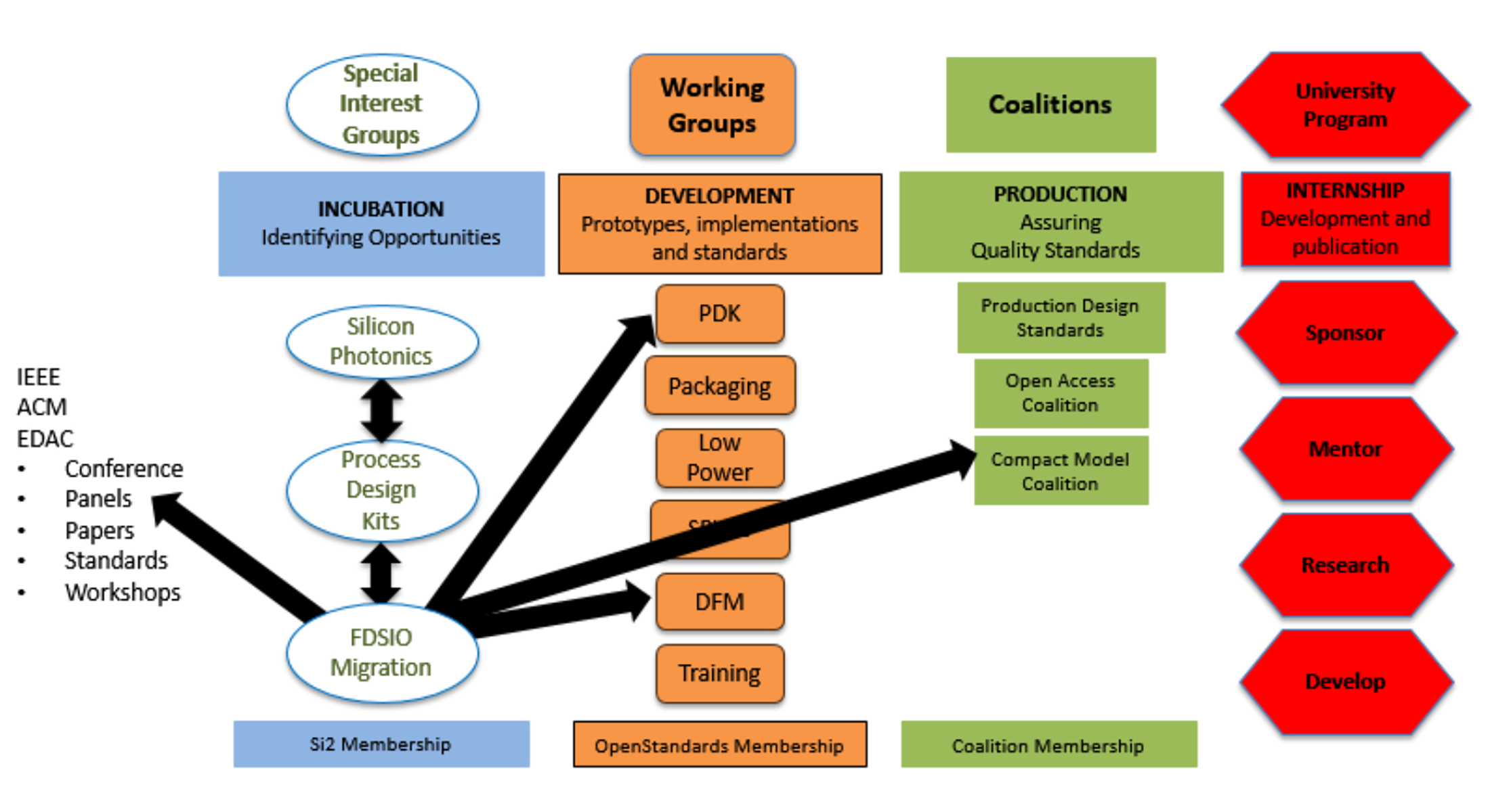
A special interest group gathers the information and incubates the ideas. The multiple SIGs share their expertise. These ideas feed additional groups through papers, standards, workshops and project and prototype requirements. Project implementation is performed by members themselves or through the Si2 Working Groups under OpenStandards with the support of the working group members. The working groups spring up to complete a project, and the results are available to working group members. Some of the projects directly affect production design standards coalitions, OpenAccess and the Compact Model Coalition. Graduate and undergraduate students participate in development under the mentorship of the SIG and working group members to create the standards and implementations and supporting information. All this is done under the protection of Si2.

Si2 primary mission is identifying common problems and providing paths to solutions. Starting with the Special Interest Groups, the Si2 structure efficiently extends the industry’s resources, enabling collaborative development while protecting proprietary IP. What can we help each other with today?

________

Si2 is a research and development joint venture that provides collaborative research and development leading to accelerated interoperability solutions and standards. As defined by the National Cooperative Research and Production Act of 1993, activities conducted under the auspices and guidance of Si2 receive a large measure of protection against federal anti-trust laws.